0

I am designing a two stage push-pull class B audio amplifier with s 2N4401 used as my pte-amplifier stage and TIP31C & TIP32C as my push-pull stage where my RL is a 10W speaker.

I am trying to set both my pre-amplifier stage and push-pull stage to be 30V VPP or at least push-pull, but I am unable to obtain those results no matter how many times I calculate. Also, I am still not sure about my diodes (1N4001) since I might replace them with a 10k potentiometer.

These are my calculations done via MATLAB:

%% First Stage 
R1= 50; R2= 20E3; R3= 1.45E3; R4= 196; R5= 11.5;
B= 300;
C= 10E-6;
F= 6E3;
Vs= 0.7;
Vcc= 30;
XC1= (1./(2*pi*F*C));

R6= 1E3; R7= 1E3; RL= 8; B2= 50; Vd1=0.7; Vd2=Vd1;

%DC Analysis VB= Vcc(R3/(R2+R3)); VE= VB-0.7; IE= (VE/R4); re= (25E-3/IE); Rin= ((1/R2)+(1/R3)+(1/(B(R5+re))))^-1; Rb= ((1/R2)+(1/R3))^-1; Ieq=(VE)/((Rb/(B+1))+R5); Vce= Vcc-(Ieq*(R4+R5));

%AC Analysis Gain= (R4/(R5+re)); Vout= Vs(Rin./realsqrt((Rin+R1)^2+(XC1).^2))Gain; Gaindb= 20*log10(Vout/Vs);

FC= (1/(2pi(R3)*C)); %% Second Stage

%DC Analysis It=(Vcc-Vd1-Vd2)/(R6+R7); %if I have diodes in the middle %It=(V2-(-V3))/(R7+R8+R10); %if I have resistor in the middle Vb1=Vcc-(It*R6); Vb2=Vb1-(Vd1+Vd2); %Vb2=-Vb1; %no diodes Ve1=Vb1-0.7; Ve2=Ve1; Vceq1=Vcc/2; Vceq2=Vceq1;

%AC Analysis Rinpp=((1/R6)+(1/R7)+(1/(B2(RL))))^-1; Vout2=Vout(Rinpp/(Rinpp+R4));

Updated My circuit:

enter image description here

JRE
  • 71,321
  • 10
  • 107
  • 188
  • There is something called a vbe-multiplier, which is commonly found instead of D1 and D2. Would that be unacceptable? Also, you are hitting on 15 W output, which is bordering on non-trivial. (Heat will certainly now be an issue.) I have read an earlier question (maybe two) but I'm not sure what this is about. Part of a process of education? Or? And your 1st stage is almost never used in cases like this. In fact, the one you show is to be specially discouraged. Are you open to considering differing approaches? Or locked into that one? – jonk Jun 05 '22 at 18:11
  • You say you are using a 10 W speaker but are demanding +/- 15 V at the output of your driver, which is closer to 15 W (given the 8 Ohm load I see.) You may want a bigger speaker or a smaller specification that fits the speaker you have. And again, is this an exercise for simulation? Or do you plan on trying your hand at building this? And after all this, you aren't really asking a question so much as "any help would be appreciated." (Kind of like throwing mud at the wall to see what sticks there.) You may want to take learning about these things in steps. – jonk Jun 05 '22 at 18:23
  • 1
    To get 10W across 8-ohm resistor you need a peak voltage to be equal $V_L = \sqrt{210W8\Omega} \approx 12.7 Vpeak$. This means you need a 25.4V peak-to-peak. Thus, your supply voltage is too low. What about the load current? ILpeak= 12.7V/8Ω = 1.6A. The $\beta$ of TIP31 will be at best around 50. Thus, the base current needed is equal to 32mA. So, for sure R6 = 2kΩ will be unable to provide such a large current. – G36 Jun 05 '22 at 18:36
  • Also, your first stage will be unable to drive such a demanding load. And no one uses this topology to drive the push-pull stage. We are using the "current driven technic" to drive the push-pull stage, not the voltage. See the example here: http://www.ecircuitcenter.com/Circuits_Audio_Amp/Advanced_Amplifier/Advanced_Audio_Amplifier.htm – G36 Jun 05 '22 at 18:39
  • http://www.ecircuitcenter.com/Circuits_Audio_Amp/Basic_Amplifier/Basic_Audio_Amplifier.htm – G36 Jun 05 '22 at 19:06
  • Your circuit is missing the AC and DC negative feedback used in all audio amplifiers. Why do you have C4? The 100uF output capacitor feeding an 8 ohm speaker cuts all low frequency bass sounds. Didn't you post this circuit on another website forum? – Audioguru Jun 05 '22 at 23:29
  • @jonk I did apply rubber diode in another circuit but I don't know how to calculate the exact value of the resistors. I tried it by using 1k both side. I might consider to different approach as long I can run 10W Speaker, but is it possible with the same design? – Sabretooth 2438 Jun 06 '22 at 04:50
  • @Sabretooth2438 I think I wrote something on the topic here. Vague recollection. It was ages ago. But it does seem to still be around. Also, you still need to address some of the questions I posed. I'd like to hear some of your thoughts. – jonk Jun 06 '22 at 04:54
  • @jonk I will be building with hands on speaker once I finalized the design ,isn't +/- 15V = 10Vrms? – Sabretooth 2438 Jun 06 '22 at 04:57
  • @G36 so Approximately 9 Vrms is needed correct? but is it possible to have that high values in second stage since I can't go more than 10 vrms or it start clipping – Sabretooth 2438 Jun 06 '22 at 05:01
  • @Audioguru I was trying to see if C4 could help with clipping issue that I am facing if I hypothetically put my gain as 11 and calculate it. – Sabretooth 2438 Jun 06 '22 at 05:02
  • @jonk can I use BC547C as my transistor for VBE multiplier? – Sabretooth 2438 Jun 06 '22 at 05:04
  • @Sabretooth2438 Yes, you can use the BC547C for the VBE multiplier. And you can compute, lacking the overhead voltages required for driving the beast, the required (+)/(-) rails by $\sqrt{2\cdot R\cdot P}$. In your case, this is just as G36 wrote above. Then you have to add another volt or two of overhead (depending) in order to finalize the voltage rails. If all you need is 10 W then a 30 V separation is probably sufficient. – jonk Jun 06 '22 at 05:07
  • @G36 is it possible to have one transistor in preamp stage since we don't have that much transistors available – Sabretooth 2438 Jun 06 '22 at 05:09
  • @Sabretooth2438 You probably cannot have just one transistor prior to the output stage. In any case, you are already considering a BJT for the VBE multiplier. So I don't see why you should skimp on the input stage at this point. You just need to find the transistors you need. Not quibble over how to get things to work with just one BJT at the input stage. (Besides, you very much DO need NFB for this. And that very likely means another BJT. Sorry about that. But likely true.) Basically, you want at least 5. More if possible. – jonk Jun 06 '22 at 05:12
  • @jonk by 30V separation you mean that I use different power source for the push-pull stage? also by having one power source is it dividing the voltage? aren't both of them parallel? sorry for the lots of question

    I didn't mean to skimp it just the transistor I am using it is in huge quantity or for the NFB I need PNP transistor?

    – Sabretooth 2438 Jun 06 '22 at 05:13
  • @Sabretooth2438 I just mean from the top rail to the bottom rail. If you have only one supply, then this is from the (+) rail to ground. If you have a bipolar supply then it is the difference between the (+) and (-) rails. You are sounding a bit behind the curve, though. Just FYI. This suggests to me that you've a lot left to learn. – jonk Jun 06 '22 at 05:14
  • @jonk +/15 volts both sides correct? – Sabretooth 2438 Jun 06 '22 at 05:16
  • @Sabretooth2438 If I'm reading you right, then yes. That's right. – jonk Jun 06 '22 at 05:17
  • @G36 You mentioned that if I want to lower my RL I need to increase the beta of Q4 and Q5. but the transistors I will be using have the max beta of 50. is there other way to not have any clipping and have 9 volts? did I miss something in your explanation? – Sabretooth 2438 Jun 06 '22 at 10:19
  • FYI, of all the transistors I tested, these TIP42 (close enough) had by far the worst behavior in a class AB output stage. Also you need drivers, otherwise your output current wil be limited to current through RC3 times hFe of top output transistor, which won't give you much output... – bobflux Jun 06 '22 at 12:02
  • Ahso hFe of your TIPs falls off at 2A, and safe operating area isn't enough for a 8R speaker load at 30V supply. Audio amps using these normally have several pairs. – bobflux Jun 06 '22 at 12:06
  • Most comments are for the replaced old schematic. The updated schematic uses a 4k ohms RC3 base resistor for the output transistors that limit the max peak output current to almost nothing. If 200 ohms is used then the max peak output current will be about 1.05A producing a peak output power of only 8.8W. The little 2N2222A will overheat so a larger driver transistor should be used. I agree that instead of heating a larger driver transistor then the next circuit using Sziklai pair outputs with its bootstrapping can be used. – Audioguru Jun 06 '22 at 20:11

1 Answers1

4

If you really want to get this 10W you need a drive stage between the output stage and voltage amplifier stage (Q3).

You could try to use this topology:

schematic

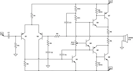
simulate this circuit – Schematic created using CircuitLab

And ballpark calculations will look like this:

Assuming \$P = 10W\$ for \$R_L = 8Ω\$

This means that \$V_{L_{max}} = \sqrt{2*P*R_L} = \sqrt{2* 10W * 8Ω} ≈ 12.7V\:\: [peak]\$

And the load current:

\$ I_{L_{max}} = \frac{V_{L_{max}}}{R_L} = 1.6A \:\:[peak] \$

For good thermal stability of an output stage, I decided to choose:

\$R8 = R9 = \frac{V_{BE}}{ I_{L_{max}}} ≈ \frac{0.8V}{1.6A} ≈ 0.47Ω \:\:[2W]\$

The output stage quiescent current (\$I_Q\$) can be set via a pot (R12) connected across VBE multiplier \$Q_8\$. And this current we need to be set on the lab bench.

\$I_Q = (2...5)\% I_{L_{max}} ≈ 50mA\$

Now if we assume \$\beta_7 = 20\$ for \$Q_6\$ and \$Q_7\$ and \$\beta_4 = 100\$ for \$Q_4\$ and \$Q_5\$ we can select \$I_{C3}\$ quiescent current.

\$ I_{C3} ≥ (5..20) * \frac{ I_{L_{max}}}{\beta_7 * \beta_4} = (5..20)* \frac{1.6A}{20 * 100}≈ 5mA\$

Due to negative feedback action, we know that the DC output voltage will be close to 0V. Thus, we can select \$R_{10}\$ and \$R_{11}\$.

\$ R_{10}+R_{11} ≈ \frac{Vcc}{I_{C3}} = \frac{15V}{5mA} = 3kΩ\$

\$R_{10} = R_{11} = \frac{3kΩ}{2} = 1.5kΩ\$

The input stage quiescent current we can find in a similar fashion, knowing Q3 DC current.

\$I_{C1} = 10 * \frac{I_{C3}}{\beta_{min}} = 10 * \frac{5mA}{100} = 0.5mA\$

\$R_2 = \frac{V_{BE3}}{I_{C1}} = \frac{0.7V}{0.5mA} ≈ 1.3kΩ\$

\$R_1 = \frac{Vcc - Vbe}{2*I_{C1}} = \frac{15V - 0.6V}{1mA} ≈ 13kΩ\$

Notice that \$R_3\$ determines the amplifier input resistance. And to reduce the "DC offset" \$R_5\$ should be equal to \$R_3\$

\$R_3 = R_5 = 10kΩ\$

\$R_4\$ will set the amplifier voltage gain.

\$R_4 = \frac{10kΩ}{10} ≈ 1kΩ\$ (gain equals to 10)

Input capacitor and C2 w set the low-frequency corner frequency

\$C_2 = \frac{0.16}{R_4 * F_C} = \frac{0.16}{1kΩ * 10Hz} ≈ 22μF\$

\$C1 = \frac{0.16}{R_3*F_C} = \frac{0.16}{10kΩ*10Hz} ≈ 2.2μF\$

\$C_C = 10pF\$ but we select the correct size of this capacitor by testing it on the test bench.

The bootstrapping capacitor: Bootstrap in power amplifier

\$C_3 = \frac{0.16}{R_{10}||R_{11} * F_C} ≈ 22μF \$

The average power dissipation in the output stage transistor (in Q6 and Q7) is equal to:

\$P_{D} ≈ 0.1*\frac{V_{CC}^2}{RL} = 0.1*\frac{15V^2}{8Ω} ≈ 2.8W\$ plus a DC current looses \$I_Q*V_{CC} = 50mA*15V = 0.75W\$

And the peak power dissipation \$P = \frac{15V^2}{4*8Ω} = 7W \$

The power in \$Q_4\$ and \$Q_5\$ is \$\frac{P_D}{\beta_7}\$. And the power dissipation in \$ Q_3\$ is \$5mA * 15V = 0.075W\$

And \$Q_8\$ (Vbe multiplier transistor) should be thermally connected with \$Q_4\$.

Now it is time to test the circuit and tweak the component values if needed. To meet the requirements.

G36
  • 14,576
  • 1
  • 20
  • 36
  • just a small question about why Sziklai transistor was used and not Darlington I am still not that well versed about them. Also, where does the pre-amplifier stage stop, and does the amplifier stage start? – Sabretooth 2438 Jun 06 '22 at 16:21
  • The main difference between Sziklai and the Darlington is that the base-emitter voltage drop (between the input and the output ) of the Darlington will be 2Vbe compared to a single Vbe drop in the Szikail pair. This circuit is a 3 stage amplifier. The input stage (Q1, Q2), the voltage gain stage (Q3), and the output stage (current gain stage) Sziklai pair. http://www.ecircuitcenter.com/Circuits_Audio_Amp/Basic_Amplifier/Basic_Audio_Amplifier.htm – G36 Jun 06 '22 at 16:41
  • is this correct? Circuit, since I am getting distorted sine wave – Sabretooth 2438 Jun 06 '22 at 17:07
  • Q4/Q5 chance to BD139/BD140 and increase Cc to 47pF. – G36 Jun 06 '22 at 17:30
  • it's fixed now, and I replaced R12 with 10 potentiometers Circuit, but in case BD139/BD140 is not available what should I substitute it with? and does this consider a class b amplifier, since it looks like Class AB? sorry for the weird question – Sabretooth 2438 Jun 06 '22 at 18:27
  • Q4/Q5 = MJE243/MJE253. And it is a class AB amplifier. But it is a very "weak" class AB ( if Iq = 50mA). Because, if the load current is larger than the 0.1A peak. The amp starts to work in class B. But If you want to be closer to class B you can reduce the output stage quiescent current from 50mA to 10mA. – G36 Jun 06 '22 at 19:05
  • Is there a way to increase my vrms to 1 and don't have clipping? – Sabretooth 2438 Jun 07 '22 at 08:10
  • Also what's maximum Vcc I can increase? Is 40 acceptable? – Sabretooth 2438 Jun 07 '22 at 08:26
  • It is obvious that if it begins clipping with an input of 0.8V RMS, a gain of 10 and a total supply of 30V then for an input of 1V RMS, the same 30V total supply and no clipping then the gain must be reduced. Do you know which resistors set the gain? Look at the datasheet of the output transistors to see if they will survive a 40V total supply and the increased heating. – Audioguru Jun 07 '22 at 13:02
  • I adjusted some values according to my transistor values, Circuit, but I want to know is there a way to increase the efficiency of the circuit? for example (efficiency=(pout/pin) *100) I get an average of 60% but want to increase it to 70% at least without clipping while maintaining my voltage on RL – Sabretooth 2438 Jun 07 '22 at 17:53
  • The efficiency is not constant but it will depend on the input voltage level. And to increase the efficiency you could try to reduce the quiescent current. Or change the circuit topology. – G36 Jun 07 '22 at 20:24