20

The Motorola 68000 has sixteen integer registers, which was considered a very generous complement at the time it was introduced. They are divided into address and data registers, eight each. Many instructions work the same with both kinds, but there are some instructions or addressing modes that only work with address registers, and some that only work with data registers.

Presumably this division saved some resources (relative to the common practice in later CPUs of making all integer registers fully general-purpose). I'm interested in exactly what resources were saved.

In particular, was it just about instruction bits, or was there a saving in wiring and multiplexer gates from only needing to connect some of the functional units to half of the registers instead of all of them?

rwallace
  • 60,953
  • 17
  • 229
  • 552
  • 2
    also setting an address register to some value doesn't affect NZVC flags. – Jean-François Fabre Sep 07 '20 at 18:27
  • 3
    Saving resources may have been one effect, but I don't think that it was the reason why it was done: In 1979 there was no CPU having "generic" registers; all CPUs on the market had registers whose purpose was dedicated. On the x86 CPUs you'll still find the dedicated purpose in the name: edi = Extended Destination Index; cl = Counter Low. So I think the 68000 designers simply didn't think about "generic" registers. – Martin Rosenau Sep 08 '20 at 05:08
  • 3
    @MartinRosenau On the contrary, the PDP-11 had mostly general-purpose registers, only R7 (the Program Counter) was special. It's often said that the 68000 was heavily inspired by the PDP-11. – Chromatix Sep 08 '20 at 06:11
  • 1
    @MartinRosenau In 1979 there was no CPU having "generic" registers except the PDP-11, the VAX-11, the DEC-10, the IBM 360/370...... I think you are probably correct with respect to microprocessors though. – JeremyP Sep 11 '20 at 10:52
  • 1
    @JeremyP I should not have written "CPU", but "microprocessor": I knew that "minicomputers" (like the PDP-11) had "generic" registers long before microprocessors were invented. However, it seems to me that many features of those machines (such as "general registers") were first used in (commercial) microprocessors much later (e.g. in the ARM-1). – Martin Rosenau Sep 11 '20 at 15:54
  • 1
    @MartinRosenau I've been unable to locate any microprocessor architectures that predate the 68000 and also have a general register file. Its ISA was far better than its competitor, the 8086. It's a bit of a shame really that the x86 architecture won in the desktop computer stakes. – JeremyP Sep 17 '20 at 08:58
  • @JeremyP It is said that IBM intentionally used the worst CPU because they didn't want to build PCs that would be able to replace IBM's more powerful (and more expensive) computers. – Martin Rosenau Sep 17 '20 at 16:43
  • 1
    @MartinRosenau I think it's more likely because of the packaging of the 8088 that allowed it to use existing external chips. – JeremyP Sep 26 '20 at 10:00

2 Answers2

29

Each of the 68K series CPUs had dedicated address-generation hardware which was wired more directly to the A registers and had only limited access to the D registers. Conversely, the main ALU was more directly wired to the D registers than the A registers. It thus became a performance enhancement, allowing the main ALU and the addressing logic to operate in parallel without conflicting in the register bank.

68000 floorplan

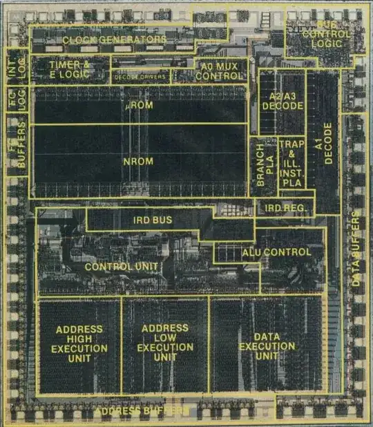
In the above die-shot with the sections helpfully labelled, you can clearly see there are separate sections of the chip for processing addresses and data. Notice also that there is no section marked "register bank"; the registers are physically entwined with their respective execution units.

In the 68040 and 68060, these separate execution units became distinct stages in the CPU's pipeline(s). The EA (Effective Address) was calculated in two stages, whose use was repeated as necessary for some of the more complex addressing modes, and the main ALU existed in another pipeline stage which came after these.

If you carefully examine the 68K instruction set, you should notice that actually, instructions which modify the A registers have different mnemonics than those for the D registers, even when they perform the same function. They decode to completely different sections of the microcode ROM (marked µROM in the floorplan) which activate the appropriate parts of the correct execution unit.

Both sets of instructions have access to addressing modes (selected by the six-bit field at the right-hand end of the instruction word) that include using either A or D registers as the second operand. Addressing modes that refer to memory are all based around A registers, with only indexed modes permitting the use of a D register in the address equation. Indexed modes take correspondingly longer, as they require an access cycle across an internal bus bridging the two execution units.

This duplication of circuitry stands in direct contrast with simpler CPUs such as the 6502 family, in which the same ALU was used for both accumulator and address-indexing arithmetic, including relative branches. Only address operations which required merely an increment or decrement (such as advancing the program counter) had logic separate from the main ALU to increase internal parallelism at minimal cost.

Chromatix
  • 16,791
  • 1
  • 49
  • 69
  • 1
    Is that a 68000, or something like a 68020? Execution times for the 68000 suggest that it uses a 16-bit ALU for both address and data calculations. For example, if memory serves, "ADD.W D0,D1" would take 4 cycles to perform a 16-bit add, "ADD.L D0,D1" would take 6 cycles to do a 32-bit add, and both "ADD.W A0,D1" and "ADD.L A0,D1" would act upon the entire 32 bits of A0, and take 6 cycles. – supercat Sep 07 '20 at 20:43
  • 2
    @supercat It's a 68000 - count the pin-pads in the address (A1-A23) and data (D0-D15) buffer sections around the edge. An '020 would have 32-bit address and data buses; an '030 would additionally have an on-board cache and MMU visible. – Chromatix Sep 08 '20 at 03:09
  • 1
    Hmm... if the 68000 has a 32-bit ALU for addressing, I wonder why the ADDA takes longer than ADD with a 16-bit D register? – supercat Sep 08 '20 at 03:32
  • 1
    @supercat It has to pull the contents of the D register over a 16-bit internal bus. You might get a better level of parallelism if you look at instructions that include an addressing mode which requires calculating an address, which is what the extra hardware is intended for. However the 68000 is a microprogrammed-control CPU, so probably doesn't take full advantage of the possibilities (eg. calculating addresses for next instruction while a previous ALU op completes). – Chromatix Sep 08 '20 at 03:35
  • 1
    The 68000 can perform 32-bit move operations in the same time required for a 16-bit ALU operation. I would have thought that meant it had a 32-bit bus and a 16-bit ALU that could operate with either the top or bottom half (somewhat like the Z80 has a 16-bit bus and 16-bit inc/dec unit, but a only a 4-bit general-purpose ALU), but perhaps each 16-bit ALU operation requires using the bus twice while moving 16 bits only requires using it once, thus allowing it to MOV 32 bits in the time required to e.g. add 16? – supercat Sep 08 '20 at 05:50
  • 1
    Otherwise, what do you think about my view that the primary advantage has to do with opcode formatting? While it would be possible to have a machine with many 16-bit instructions that used four-bit register-select fields, using three-bit register-select fields saves a lot of opcode space, making much more of it available for things like MOVEQ, A-line traps, etc. – supercat Sep 08 '20 at 05:54
  • 1
    @supercat It certainly is another benefit. One that is diluted somewhat by the need to duplicate simple move and arithmetic instructions for each combination of register banks, but still allows all those addressing modes and the more complex ALU instructions to use three-bit register fields. It's a tradeoff that made a lot of sense at the time, given the need to keep a reasonably short instruction word. ARM could be more generous with an instruction word twice as long, as memory was cheaper and wider by then. – Chromatix Sep 08 '20 at 06:05
  • 1
    I something similar could have continued to be advantageous on the Thumb if some address-select fields had mapped the eight registers selections to e.g. 0,1,2,3,8,13,10,11. The biggest problem with such a scheme is that it makes it awkward for an ABI to simultaneously support both register-based argument passing and the invocation of non-prototyped variadic functions. On non-floating point ARM, the first 128 bits of arguments are passed in R0-R3, always, without regard for whether they represent numbers or pointers. On a processor with separate address/data registers, ... – supercat Sep 08 '20 at 14:59
  • 1
    ...it would be difficult for a compiler generating the entry code for something like printf to know whether to stack the register used to pass the second pointer before or after the register used to pass the first number. Perhaps a platform could use a name-mangling convention so that C callable functions' names indicate the order of pointer, integer, and floating-point arguments, and a compiler generating code for a variadic function could generate multiple entry points, but linker philosophies seem stuck in the 1970s. – supercat Sep 08 '20 at 15:13
  • Noting @Chromatix's comments, but there's also the issue of internal signal fanout: minimising this reduces the need for internal buffers/drivers hence reduces propagation delay. – Mark Morgan Lloyd Sep 09 '20 at 07:52
  • Can anyone explain the difference between the image in this answer and the images at https://cpumuseum.jimdofree.com/cpu-die-photography/motorola/ which seem to be completely different? This image is apparently from om BYTE magazine, May 1983, "Design Philosophy Behind Motorola's MC68000" by Thomas Starnes of the Motorola team. – jonathanjo Mar 21 '23 at 01:02
7

The primary advantage of the 68000 segregating address and data registers is the ability to have many instructions use three-bit register-select fields, thus saving opcode space compared with using four-bit fields. IMHO, the ARM Thumb instruction set and derivatives could have benefited from employing such a concept, since otherwise the upper registers end up being much more awkward to use than the lower ones.

supercat
  • 35,993
  • 3
  • 63
  • 159
  • 2
    Works nicely for compiler code generation too as addressing expressions share data (e.g., across loop iterations and across both directions of an if-statement) separately from data expressions (where you're doing arithmetic on values, looking into strings for characters, transforming strings, etc.). Thus it can make sense to do register allocation separately for address calc vs data calc. And that's also why indexing allowed the use of D registers (mentioned by Chromatix in his answer): the index value is frequently (not always) the result of some data-side computation. – davidbak Sep 08 '20 at 19:14
  • 2
    @davidbak: Situations where indexing would use one address and one data register would seem much more common than those where it would require two of either sort. The biggest code-generation problem is allowing functions to efficiently receive arguments in registers, but also be able to handle both printf("%d %s", 4, "Hey"); and printf("%s %d", "Hey", 4); even when no prototype is in scope. Even that could be accommodated with name mangling and stubs, but I've never seen an implementation use such an approach. – supercat Sep 08 '20 at 19:39