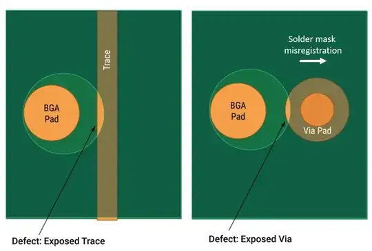
I am looking to have a PCB produced for a personal project of mine. I have to use very thin traces and tight clearances to escape pads on a BGA chip on my board. I was looking at the capabilities of JLCPCB, and noticed that they differentiated between the clearance of a pad to a wire (which they state is 0,2 mm) and clearance of a wire to another wire (which they state is 0,09 mm).
My question is: why are these numbers so wildly different? As far as I understand, they are both just pieces of copper which get selectively etched away. On some forums, I saw some people state that they ignore the pad-to-trace clearance and just take the trace-to-trace clearance. But it makes me wonder why the PCB manufacturer sees the 2 as different things.
I took the clearances from here btw.
