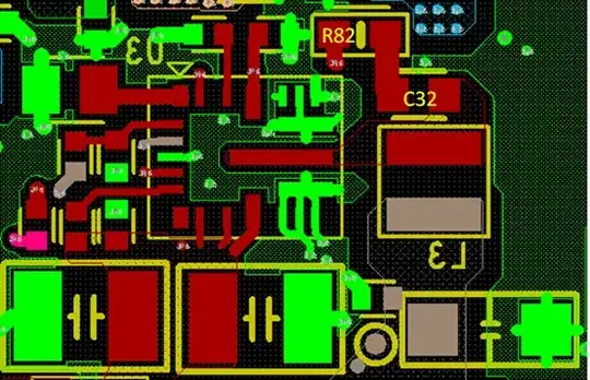
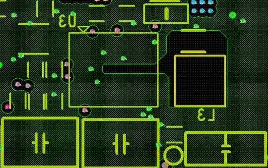
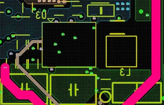
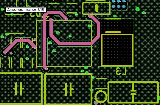
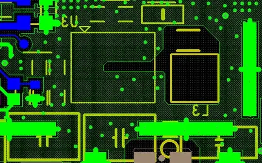
I am starting to update PCB layout to next version because EMC test result failed. As result of test, the designed Buck IC layout seems have the improvement room and noise is from 2.1MHz harmonic.
The designed Buck IC: LM53625LQRNLTQ1(2.1MHz
Test requirement:CISPR25 level 3
Test Voltage: 24V
Current layout: CE_C Pass, RE fail
Layer 1
Layer2
Layer3
Layer4
Layer5
Layer6
The information from co-worker, they used to pour copper under Buck IC and inductor form layer1 to layer6 and RE has a lot of improvement but CE_C became very bad
I would like to do a little bit modification based on current layout
Remove copper under C32 and R82 from layer1 to layer6
Pour copper under buck IC like layer 2 at layer3
my Question as below:
Why to remove GND copper of layer3 at current layout? do anyone have a kind of experience for this
I read some of buck Layout recommendation for reducing EMI
https://electronics.stackexchange.com/questions/503308/buck-converter-pcb-planes>
but there is no article to be discussed with how to pour copper under switching node and Buck IC.
