I am very much a novice w/ electronics. I'm trying to evaluate these risers for use in a system where I need to add additional GPUs and a 2nd PSU (the first PSU is 1600W and maxed out w/ 4 GPUs, the CPU, etc.). I'm not using the system for mining and need as much PCIe bandwidth as I can get, which rules out the low cost, x16 to x1 risers which allow for power isolation. There are eGPU risers which go from x16 to x4 which I suppose I could settle for if this riser is risky.
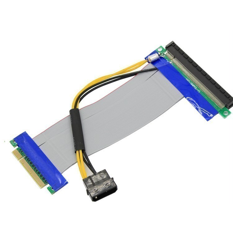
Is it correct to say this riser would feed 12V from the new PSU over the molex/peripheral connector, cutting off the 12V which would have come from the original PSU over the PCIe slot? Or is it just meant for additional power?
Is the capacitor meant to filter the 12V coming from the 2nd PSU? Or is it meant to bridge some presence detect pins?
Is this a reasonably safe way to do this, assuming a good job was done fabricating/soldering everything together?
The PCIe slot still provides 3.3V at up to 3A, which is passed through by this riser. Why is this not an issue in terms of the 2 PSUs? Is it because there is typically some kind of isolation on a graphics card between the 12V and 3.3V lines/circuits? If so, how can one know in advance whether a particular card does this without having to physically try it?
There is also these powered risers, which mention they 'add additional power' but seem to have additional circuitry beyond the ones I linked above. Are these a better alternative for power isolation between the 2 PSUs?
EDIT:
The question I asked is a bit too specific to these non-standard products so let me clarify (w/ another non-standard product ;)).
Let's say I have a PCB w/ a PCIe x16 slot and a circuit as shown below. I found the schematic here. It looks like it's taking in 12V from an 8-pin PCIe connector (JP1), feeding it through a power MOSFET (Q1) and then feeding it to the card (+12vPCIE). It also uses a DC-DC converter (U1; part # TPS564201DDCT) to generate 3.3V for the card as well.
There are 4 individual connectors, each of which would connect to an LVDS cable providing 4 PCIe lanes. These cables would connect to some separate PCB which would plug into a PCIe slot on the system. One of the cables seems to provide 3.3V from the motherboard (+3.3v_Host).
My question is does this circuit seem sound? Is there anything glaring/obvious to change? From my perspective:
- There's a fuse
- The power MOSFETs (datasheet) continuous drain current @ 70C is shown as -16A. Is this the right field to look at for knowing how much current this MOSFET can handle?
- The 8-pin PCIe connector is rated up to 150W (3 12V lines each capable of ~4A) which should be enough since the 12V rail on PCIe slots only draws up to ~5.5A/66W (+ 3A @ 3.3V) or a total of ~75W
- The 3.3V from the host doesn't seem to really provide any real current and as I understand it just turns on/off BJTs? (does this mean its 'power isolated'?)

If it's sound and I can find the corresponding cables and associated adapter I'm wondering if it would be a good idea to have this fabricated.
Thanks for any help/suggestions