Short answer: No.
Longer ...
Use: Vdd = Vcc.
See my recent answer about protection diodes on IC pins.
Each pin has a (usually) reversed biased internal "protection" diode from pin to Vdd. Removing power to Vdd will cause it to drop to close to ground potential. Voltage applied to other pins will be conducted to Vdd via the pin's diode. From there "anything can happen and something may". Results are not predictable. Some IC's can be powered that way. Some people have built circuits that have no apparent power source but which are purposefully powered by a protection diode. This can be 'fun" to do but is bad practice and unexpected results can be expected.
HOWEVER, it would be useful to know what you are trying to achieve. If it is only to get a 1 of N output selector, this can be done by using N/10 x 4017's and enabling one at a time, using one extra IC as a selector. CD4107 data sheet at [1] (below).
See block diagram on page 2 of datasheet. Pin 13 is a negative active clock enable input, pin 12 is a clock output signal and pin 15 is an active high reset line. These may be used in a number of ways to create a multi IC one of N selector. As you were intending to sequentially select Vdds you can instead just select enable and reset lines. Note that as clock enable is true-low and reset is true-high, typing clock-enable and reset together gives you a single control signal which allows counting when low and which both clock-disables and resets the IC when high. That should be enough to allow a design, but the following suggests one method.
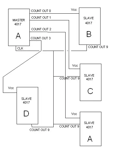
If 2 x 4017's (MA. MB = masterA masterB) are connected in series with clock to MA clock, carryout of MA to clock of MB, then the outputs of MB will successively go high for 10 clock cycles. The MB outputs can then be used to enable slave 4017's SA, Sb Sc ... . Up to 100 outputs can be obtained this way giving 10N outputs using N+2 x 4017s.
If less than 10 x slave 4017s are used the carryout signal from the last slave can be used to reset the counter chain.
Note that MB's outputs are active high , which is the wrong polarity to directly drive either slave rest lines or slave clock enable lines. An inverter would be require from each MB output to the matching Sx clock enable line.
There are other 1 of N output IC's and other ways of doing this. If you can advise the number of outputs required and what is being driven then a better answer can be provided. A cheap microcontroller with many port pins may be the best solution. If a microcontroller is used to drive this chain other IC's may be appropriate.
A one of N IC with active low outputs would eliminate the need for inverters in the Sx clock-enable lines.
Using the output of slave Sn to reset the system to initial state risks a "race hazard". A little thought re timing of the rest pulse may be requried to ensure clean reset.
More if required ... .
[1] http://media.digikey.com/pdf/Data%20Sheets/Fairchild%20PDFs/CD4017BC,%20CD4022BC.pdf
.